
1. Context
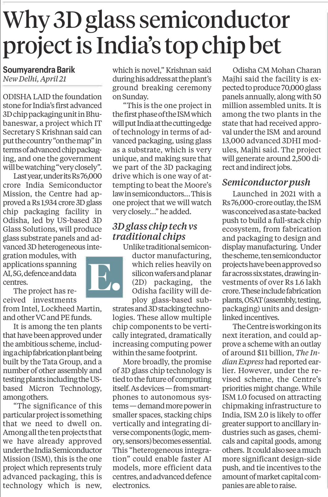
- India has made a strategic entry into advanced semiconductor technology through 3D glass-based chip packaging, moving beyond basic assembly into a high-value, next-generation segment of the global chip value chain.
- This is positioned as a key technological leap for applications like AI, telecom, and data centres.
2. 3D Glass Chip vs Traditional Chip
- Traditional (2D chips): Horizontal layout on silicon → limits scaling, higher heat, slower data transfer.
- 3D glass chips: Vertical stacking using glass substrates → faster, energy-efficient, better heat management, higher density.
- Key shift: 2D planar → 3D integrated architecture.
3. India’s Semiconductor Mission
- The India Semiconductor Mission was approved in 2021 under the Semicon India Programme.
- Outlay: ₹76,000 crore (initial), with expansion in later phases.
- Objectives:
- Reduce import dependence
- Build a self-reliant semiconductor ecosystem
- Position India in global supply chains
- Focus Areas:
- Fabrication (fabs)
- ATMP (assembly, testing, packaging)
- Chip design and R&D
- Advanced packaging (like 3D glass technology)