
Context: India Semiconductor Mission 2.0
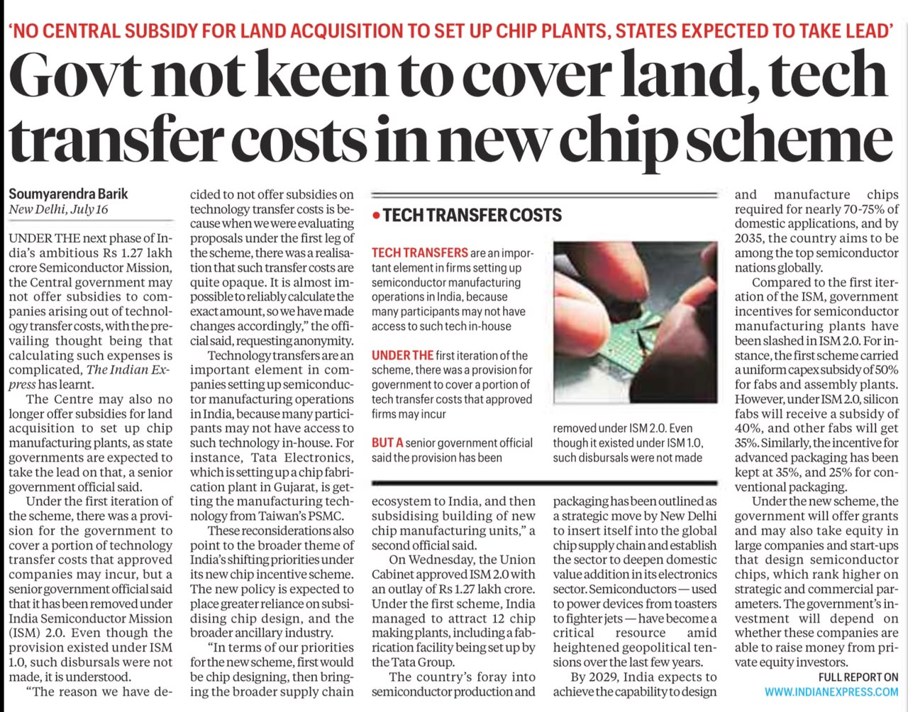
The Union Cabinet has approved India Semiconductor Mission 2.0 with an outlay of ₹1.27 lakh crore.
Compared to ISM 1.0, the new scheme proposes no Central subsidy for land acquisition and technology transfer costs, with States expected to provide land.
The policy shifts focus towards:
- Chip design
- Domestic value addition
- Complete semiconductor ecosystem building
India Semiconductor Mission
Launched
2021
Nodal Ministry
Ministry of Electronics and Information Technology.
Objective
To develop an end-to-end semiconductor ecosystem covering:
ATMP / OSAT
ATMP means Assembly, Testing, Marking and Packaging.
OSAT means Outsourced Semiconductor Assembly and Test.
Target
India aims to meet 70–75% of its semiconductor demand by 2035 and emerge as a leading global semiconductor hub.
What Changes in ISM 2.0?
1. No Land Subsidy
The Centre will not provide subsidy for land acquisition.
States are expected to arrange land for chip projects.
2. No Technology Transfer Cost Support
Technology transfer costs have been removed from eligible incentives because these costs are difficult to assess transparently.
3. Reduced Capital Subsidy
Compared to ISM 1.0:
- Silicon fabs: 50% to 40%
- Other fabs: 50% to 35%
- Advanced packaging: 35%
- Conventional packaging: 25%
4. Support for Design Companies
Government may provide grants and equity support to semiconductor design companies, subject to their ability to attract private investment.
Why This Policy Shift?
1. Chip Design First
The policy prioritises chip design before manufacturing and supply-chain development.
2. State Participation
States are expected to play a greater role in infrastructure creation.
3. Domestic Value Addition
The focus is on long-term domestic value addition rather than subsidising opaque one-time costs such as technology transfer.
Significance
- Strengthens semiconductor ecosystem.
- Encourages private investment.
- Promotes chip design capacity.
- Supports electronics manufacturing.
- Reduces import dependence.
- Builds strategic technological capability.
Key Takeaway
ISM 2.0 shows a shift from broad subsidies towards a more ecosystem-focused semiconductor strategy based on design, domestic value addition and State-led infrastructure support.